- 您现在的位置:买卖IC网 > Sheet目录2001 > ISL5729/2INZ (Intersil)IC DAC 10BIT CMOS DUAL 48LQFP
4
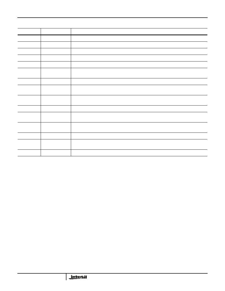
Pin Descriptions
PIN NO.
PIN NAME
PIN DESCRIPTION
11, 19, 26
AGND
Analog ground.
13, 24
AVDD
Analog supply (+2.7V to +3.6V).
28
CLK
Clock input.
27
DGND
Connect to digital ground.
10
DVDD
Digital supply (+2.7V to +3.6V).
20
FSADJ
Full scale current adjust. Use a resistor to ground to adjust full scale output current. Full scale output
current = 32 x VFSADJ/RSET.
14, 23
NC
Not internally connected. Recommend no connect.
12, 25
ICOMP, QCOMP
Compensation pin for internal bias generation. Each pin should be individually decoupled to AGND with
a 0.1
F capacitor.
1-4, 29-38,
43-48
ID9-ID0, QD9-QD0
Digital data input ports. Bit 9 is most significant bit (MSB) and bit 0 is the least significant bit (LSB).
15, 22
IOUTA, QOUTA
Current outputs of the device. Full scale output current is achieved when all input bits are set to binary 1.
16, 21
IOUTB, QOUTB
Complementary current outputs of the device. Full scale output current is achieved on the complementary
outputs when all input bits are set to binary 0.
17
REFIO
Reference voltage input if Internal reference is disabled. The internal reference is not intended to drive an
external load. Use 0.1
F cap to ground when internal reference is enabled.
18
REFLO
Connect to analog ground to enable internal 1.2V reference or connect to AVDD to disable internal reference.
5-8, 39-42
NC
No connect (NC). Not internally connected. No termination required, may be used for device migration to
higher resolution DACs.
9
SLEEP
Connect to digital ground or leave floating for normal operation. Connect to DVDD for sleep mode.
ISL5729
发布紧急采购,3分钟左右您将得到回复。
相关PDF资料
ISL5757IBZ
IC DAC 10BIT 260MHZ 28-SOIC
ISL5761/2IBZ
CONV D/A 10BIT HS LP 28-SOIC
ISL5827INZ
IC DAC DUAL 12BIT 3.3V 48-LQFP
ISL5857IAZ
IC DAC 12-BIT 260MSPS 28-TSSOP
ISL5861/2IBZ
IC DAC 12BIT 210MSPS 28-SOIC
ISL5927INZ
IC DAC 14BIT CMOS DUAL 48LQFP
ISL5929INZ
IC DAC 14BIT CMOS DUAL 48LQFP
ISL5957IBZ
CONV D/A 14-BIT 3.3V 28-SOIC
相关代理商/技术参数
ISL57292IN
制造商:INTERSIL 制造商全称:Intersil Corporation 功能描述:Dual 10-bit, +3.3V, 130/210MSPS, CommLink TM High Speed D/A Converter
ISL5729EVAL1
功能描述:EVALUATION PLATFORM FOR ISL5729 RoHS:否 类别:编程器,开发系统 >> 评估板 - 数模转换器 (DAC) 系列:CommLink™ 产品培训模块:Lead (SnPb) Finish for COTS
Obsolescence Mitigation Program 标准包装:1 系列:- DAC 的数量:4 位数:12 采样率(每秒):- 数据接口:串行,SPI? 设置时间:3µs DAC 型:电流/电压 工作温度:-40°C ~ 85°C 已供物品:板 已用 IC / 零件:MAX5581
ISL5729IN
功能描述:IC DAC DUAL 10BIT 3.3V 48-MQFP RoHS:否 类别:集成电路 (IC) >> 数据采集 - 数模转换器 系列:- 标准包装:2,400 系列:- 设置时间:- 位数:18 数据接口:串行 转换器数目:3 电压电源:模拟和数字 功率耗散(最大):- 工作温度:-40°C ~ 85°C 安装类型:表面贴装 封装/外壳:36-TFBGA 供应商设备封装:36-TFBGA 包装:带卷 (TR) 输出数目和类型:* 采样率(每秒):*
ISL5729INZ
功能描述:IC DAC 10BIT CMOS DUAL 48LQFP RoHS:是 类别:集成电路 (IC) >> 数据采集 - 数模转换器 系列:- 产品培训模块:Lead (SnPb) Finish for COTS
Obsolescence Mitigation Program 标准包装:1,000 系列:- 设置时间:1µs 位数:8 数据接口:串行 转换器数目:8 电压电源:双 ± 功率耗散(最大):941mW 工作温度:0°C ~ 70°C 安装类型:表面贴装 封装/外壳:24-SOIC(0.295",7.50mm 宽) 供应商设备封装:24-SOIC W 包装:带卷 (TR) 输出数目和类型:8 电压,单极 采样率(每秒):*
ISL5740
制造商:INTERSIL 制造商全称:Intersil Corporation 功能描述:3V Dual 10-Bit, 20/40/60MSPS A/D Converter with Internal Voltage Reference
ISL57402IN
制造商:INTERSIL 制造商全称:Intersil Corporation 功能描述:3V Dual 10-Bit, 20/40/60MSPS A/D Converter with Internal Voltage Reference
ISL57403IN
制造商:INTERSIL 制造商全称:Intersil Corporation 功能描述:3V Dual 10-Bit, 20/40/60MSPS A/D Converter with Internal Voltage Reference
ISL57404IN
制造商:INTERSIL 制造商全称:Intersil Corporation 功能描述:3V Dual 10-Bit, 20/40/60MSPS A/D Converter with Internal Voltage Reference